06-4981-7658
liuting15538@gmail.com
〒535-0004 大阪府大阪市旭区中宮2丁目19-5 ルベール公園前 2階201号室


HIGH-Sc ScAIN WAFER MANUFACTURING CHALLENGES
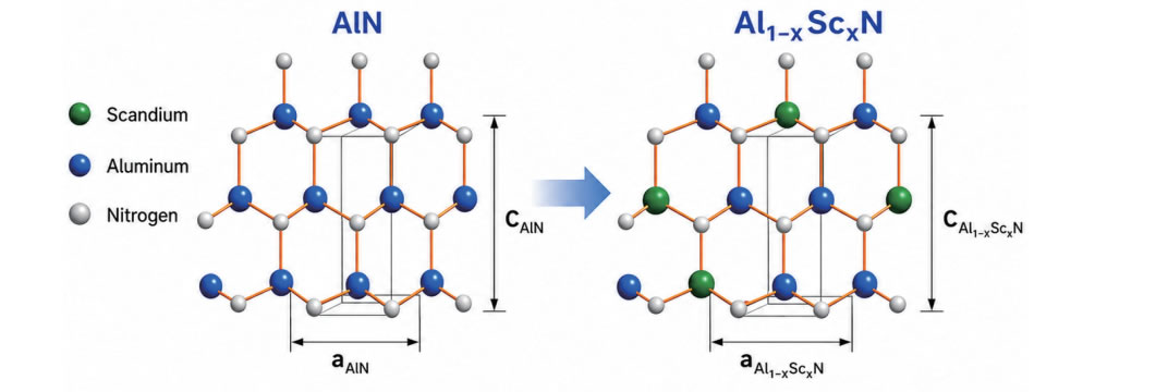
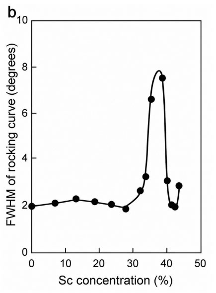
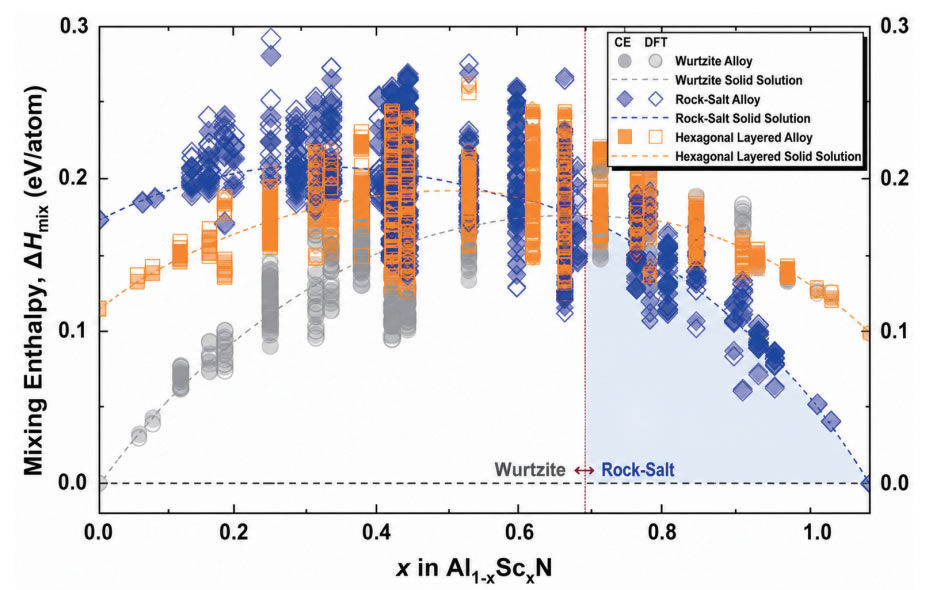
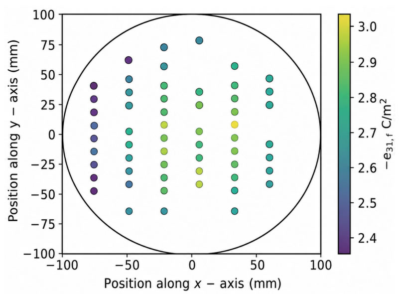
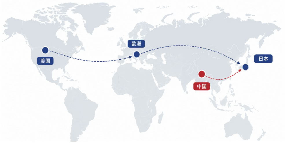
ADVANTAGES
ScAl Alloy Target
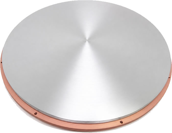
参数指标Parameter |
ScAI合金靶材ScAl Alloy Target |
|---|---|
尺寸Size |
3-14 inch |
成分Composition |
ScAl, Sc: 20-45 at% |
表面粗糙度Surface Roughness |
Ra < 1.6 um |
纯度Purity |
4N |
氧含量Oxygen Content |
< 1000 ppm |
Full-Sc-Composition ScAIN Thin-Film Process
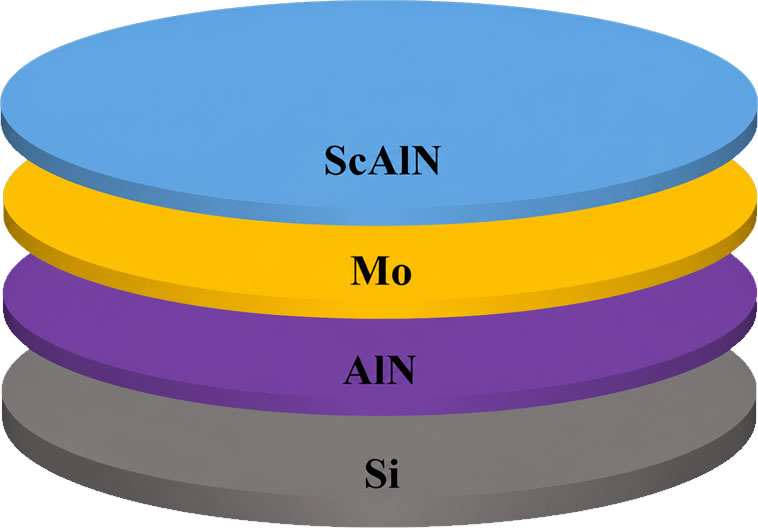
规格参数Specifications |
拓扑半导体Top Semiconductor |
|---|---|
晶圆尺寸Wafer Size |
8英寸8-inch |
Sc组分范围Sc Content Range |
5-35 at% |
ScAIN薄膜厚度ScAIN Film Thickness |
100-1000 nm |
表面粗糙度Surface Roughness |
< 2 nm (5 um*5 um) |
XRC半高宽XRC FWHM |
< 2° |
薄膜应力Film Stress |
< 1000 ppm |
薄膜均匀性100-120 MPa |
± 0.5% |
Periodically Polarity-
Reversed ScAIN Thin-Film Process
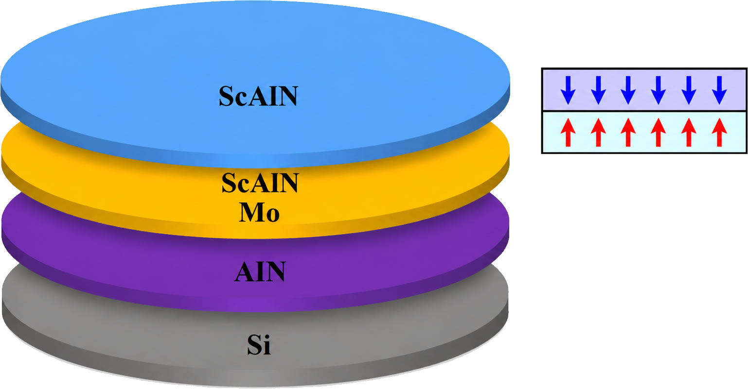
维度Dimension |
参数Parameter |
|---|---|
尺寸Size |
8英寸8-inch |
Sc含量Sc Content |
5-35at% |
周期性层数Periodic Layer Number |
> 2层 |
层间差异Interlayer Variation |
< 1% |
XRC半高宽XRC FWHM |
< 2° |
表面粗糙度Surface Roughness |
< 2nm (5um*5um) |
Domestic 8-inch ScAIN Wafer-Level
Production Platform
(Toptech Clusterline 200 Series)
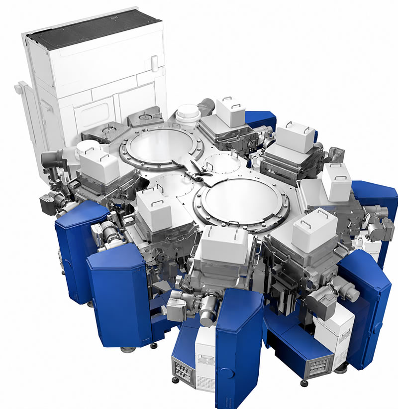
核心能力维度Core Capability |
拓扑半导体国产方案Top Semiconductor Domestic Solution |
|---|---|
晶圆尺寸Wafer Size |
8英寸8-inch |
架构形式Architecture |
Cluster集群式Cluster Type |
基础真空Base Vacuum |
< 5x10^-8Torr |
厚度均匀性Thickness Uniformity |
<±1% |
片间重复性Wafer-to-Wafer Repeatability |
< ±1% |
应力控制Stress Control |
±120MPa可调 |
靶利用率Target Utilization |
> 45% |
06-4981-7658
liuting15538@gmail.com
〒535-0004 大阪府大阪市旭区中宮2丁目19-5 ルベール公園前 2階201号室


